


Discover the video presentation of the project and its results!
connectorized SMM probe @60GHz
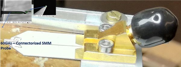
Details of a sub-50nm SMM probe integrated in a 254µm thick PCB supporting a microstrip mode with a 1.85mm connector.
This probe is part of the SMM integrated in an SEM; it operates up to 60GHz with insertion losses close to 2.5 dB at 40GHz.
What are the project developments?
Project progress
The project has now achieved its first year of activity. And a lot happened! First we can mention an excellent synergy between the partners and a strong will to work together. The partners already participated in conferences and events to present the first results of the project. On the technical side, let’s overview the different progress.
1. Development of Scanning Microwave Microscopy (SMM) technology on electrical resolution, bandwidth, and microwave probes
So far, we attain a good performance on shielded planar SMM probes up to 40 GHz and ultra-broadband (kHz – 20 GHz) SMM solutions are achieved as expected. The vertical SMM using coaxial tip is in good progress, the coaxial tip is now successfully developed with improved electrical and mechanical properties.
Until now, the work focused on design, fabrication and measurement of SMM cantilevers integrated in microstrip based PCB, to achieve 110 GHz operation. A new design has been provided with thinner substrate and smaller transmission line width.
The SMM cantilever (40 GHz) has been integrated in a microwave head and laser detection system. The whole system integrated into a Scanning Electron Microscope (SEM) has been fully automated using nano-positionning stages controlled by a computer.
A coaxial tip has been successfully developed and improve both electrical and mechanical properties.
The design and 3D electromagnetic (EM) optimization of hybrid calibration kits for simultaneous SEM, AFM and SMM calibration is achieved.
A complex impedance SMM measurement workflow has been successfully defined, when a wideband frequency AFM for kHz – 20 GHz electrical measurements has been implemented. The system operated in either tapping or lift mode to provide absolute impedance and dC/dZ.
2. Application oriented SMM and development of new calibration routines
The concept of the combined SMM/SEM has been established, allowing to run initial tests on thin samples. Then the stitching procedure was developed and fully tested on various samples, which allows increased image sizes. They showed an increase by a factor of 16 in image size, with a final implementation showing a factor of 25 increase in image size (going from 100 µm2 to 500 µm2).
SMM calibration procedures were integrated into a GUI to allow a proper inclusion into the SMM measurement workflow and SMM software. Finally a GUI was established for semiconductor dopant profiling as well as materials complex impedance.
3. Electromagnetic 3D models and software modules
Three common user cases of industrial measurement systems (MOdelling DAta representative of SMM, dielectric resonator, and coaxial probe measurement) have been agreed and defined for further simulation development. Full Maxwell electromagnetic solvers capable of solving axisymmetrical structures have been developed. Consequently the user cases have been analysed and solved by using developed simulation software based on FEM and FDTD.
A literature survey has been prepared to improve electromagnetic solvers and to develop initial semiconductor model with drift- and diffusion approach. In addition, comparison of available multiphysics solvers with and without semiconductor modelling have also been done.
4. Fabrication and characterization of reference materials and structures for validation of SMM technologies at the lab scale.
The activity covered the fabrication, physic-based characterizations and optimisation of organic photovoltaic (OPV) reference materials and composite prepegs and electrodes.
A Split Post Dielectric Resonator (SPDR) operating at 10 GHz was mounted in a scanner to investigate materials. Complementary characterization work is carried out to determine intrinsic properties (optical, electrical, morphological and structural) of the materials and structure in device environment.
Two batches of carbon-based composites followed by a batch of graphene-based electrodes were produced. Morphological and compositional characterization were carried out (SEM-EDX).
A demonstrator of a new portable 10 GHz Q-Meter was constructed in three separate scrap chassis. Regarding the study of large scale (semi-)conducting films with a dielectric resonator, the efforts concentrated on theoretically developing a new resolution improvement technique.
5. Demonstration of macro-scale microwave characterisation techniques for in-line pilot production
Partners started to study the adaptation of the GHz measurement platform (probe kit, dielectric resonator) from laboratory environment to sheet-to-sheet inline industrial application.
The first step was to design the overall dielectric resonator and coaxial probe tip solutions integration in industrial environment. As a first stage, a list of materials was defined for thin film PV modules. The second step was to detail the production process in terms of time constraint and quality expected. Finally, a benchmark of existing metrological systems for analysis in production of PV systems was performed to evaluate integration efficiency of the various solutions in complementary.
The second task consisted in performing the integration of macro-scale dielectric resonator and coaxial probe systems in pilot-line production process.
6. Development of standard operating procedures and implementation of open access environment
The definition and description of metadata to provide ample information on sample and instrument settings and thus allow reproducing measurements and provide input to simulations have been established. The definition of metadata has been as well discussed with the concerned partners and is documented in the data management plan, and the Web interface for open innovation environment has been set up.
The open innovation environment has been set up. The public level (https://www.mmama.eu/oip/) gives access to the documents which are publicly accessible according to the data management plan.
WP1: tip holder with coaxial tip (METAS)
In WP1, Development of SMM technology on electrical resolution, bandwidth, and microwave probes, METAS works on an open air vertical tuning-fork based SMM and develop an RF connection from coaxial cable to tip and develop modified microscope head:


